
In a previous post (Electronic Prototype Fabrication. Part 1: Why making electronic PCB prototype is useful) I explained why electronic prototyping is an important step in the product development process of an electronic product.
In this blog post you will learn how PCB and PCBA prototypes are made during the electronic product development phase. Normally, this phase comes once the electronic engineering is achieved. So, at this point we can consider PCB Schematic is completed, PCB Layout has been drawn and verified, Bill of Material is stabilized, Gerber files including layer, component positioning and drilling have been generated.
What are the different steps of making electronic prototype and how do we handle them
Below is a general scheme of the processes involved in creating electronic pcb prototypes. You can see there are quite a few steps and most of them got their dose of risks of failure. Astonihly, but in order to remain competitive, in 2017 we are stilling making PCB prototype by hand.
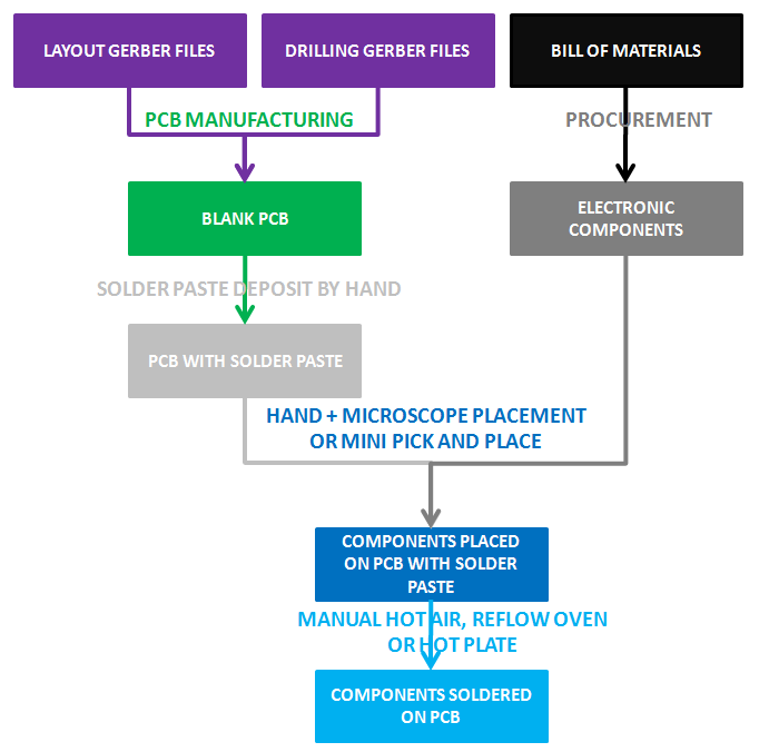
1./ Blank PCB prototype procurement
For recall, a PCB (also called “blank PCB”) is a Printed Circuit Board which doesn’t host any electronic component yet. By opposition, a PCBA also called Printed Circuit Board Assembly is a PCB on which electronics components have been soldered/assembled.
This part of the process for prototype is made the same way than for manufacturing. One of the main difference is that manufacturer will try to panalize as much as possible several design of several customers on the same plate so they can optimize their costs in terms of plate allocation.
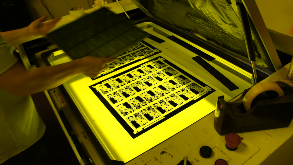
To perform this step, heavy equipment are required: several chemical bath, CNC drilling machines, CNC cutting machines, silk screen machine etc.. It uses as input the Gerber files generated by an EDA software such as Altium, Orcad Allegro, Kicad or Eagle to feed a full chain of machine creating blank PCB.
I personnaly have a database of several PCB manufacturers I have audited myself because I don’t use the same PCB manufacturer for different projects. Indeed, some PCB prototype manufacturers may be capable and competitive to make 2 layers PCB but can have difficulties to process 4 or more layers with reliability. This is particulary true when it comes to high quality PCB requiring physical adjustments such as impedance matching.
Obviously, if PCB prototype quality is not proper, then your electronic pcb prototype might not work properly either. Normally, a serious supplier would make some track testing using some flying probe to verify the tracks on the PCB. If they don’t do it, you might risk to receive some PCB with defects: you will solder your components and your board will not work properly. You will spend hours and hours finding out why and finally you will realize that problems comes from manufacturing. Quite frustrating !!!
2./ Electronic components procurement
It may sounds easy to do. You might think: “buy component? I can do, this like going to shopping !”. In reality, it can become not that easy at all depending on how the bill of material has been

established by the pcb architect and the pcb hardware engineer.
Indeed, if the hardware engineer selected components which are difficult to supply because the components is rare on the market or just outdated, then it can become a nightmare to success to find the components at decent price on the market to populate your PCB and to respect the bill of material. In some case, the components might need to be imported specifically or might need to be subsituted by another equivalent one (I recommend to avoid this, but if it is necessary then the people in charge of sourcing and procurement should ask for validation to the hardware engineer).
Another problem you may face is to buy sample components to a vendor who can also supply bigger quantities later for manufacturing with reliability, so that you can get consistency on your supply chain for your components. I see quite a lot of people who buy components in the electronic market in Shenzhen (Hua Qian Bei) to small shops. They go here and there so find some vendors selling components and buy some samples to make their prototype. Later when they want to mass produce, they have either difficulties to find another vendor more reliable for production to match exactly the same components or they need to rely on the small shop they used. Quite often the small shop will not disclose who is the real manufacturer of the component, hence you loose control on the supply chain and the shop can change the manufacturer behind your back without you know it, putting your production at risk.
Hence, when you buy components, even for sample, I recommend to buy them for reliable sources. For example, you can use Arrow or Element 14, those are big components distributor and they don’t substitute components behind your back.
I recommend to be very organized when performing components procurement because it can quickly become terrible to manage: when you got a bill of material with 100 different component references you need to make sure you got all of them and you need to make sure you don’t mix them (yes you can because sometimes components are not marked) !
I personnaly use some zip lock plastic bags on which I ad some sticker with component part number and I never put components of those bag unless I need to solder them.
3./ Assembling components on blank PCB
A./ Solder paste deposit

Now you got your components and your blank PCB in hand, you then need to solder components on pcb so they can connect with each other and realize your circuit which then you will test. If you are on SMD type configuration then it means your component will be soldered on pads and not trough hole. It means some soldering material should be placed and melt between components and PCB. So the question is how to place properly solder paste on pad properly (not too much, not too less).
Well here there are differents technics, some people do this by hand and it is very difficult. The best solution is to use what we call a laser net: this is typically a frame with a layer of aluminum being cut with a laser exactly to keep some opening on the surface of the pads. In short, it creates a canvas where the solder paste will be placed only on the pad. This frame can be placed on an automatic machine, but for prototype we mostly use manual one because we make very low quantity of prototype (usually no more than 5 pieces).
I can tell you the first time I tried to make a PCBA prototype I have attempted to use a hand solder, components and normal tin solder wire and it didn’t work at all because components are so small that it is extremly difficult to perform a clean soldering this way. I don’t mention either that soldering component with having pads below the components make impossible to solder a comopnent on a pcb with using a solder paste material.
Since then, I have my own manual laser net apparatus which I use to deposit solder paste on PCB. It gives me some ease to put exactly the necessary solder paste quantity on the right area of the PCB.
B./ Components placement
Now that you have your solder paste placed on the pcb pads you will need to place components exactly at the location of the pads so it can solder properly. This part is the most complicated part of making electronic pcb prototype. Why ? Simply because today components are so small that you can not even catch them with a tool. Now imagine you have 100 references on your bill of material, and each references got 2 components each. This is around 200 components to place on your PCB, and most of them got size around less than a millimeter length.
There are two ways to achieve this:
- Pick and Place machine or mini pick and place machine: it makes automatic placement. This can be costly because machine need to be set and ready for making only 5 pieces prototype, so the settup cost outweight the product cost. However, if the pick and place is of good brand, it should be able to place all the components properly at the right location.
- Manually: I usually do it this way. It can be quick for small PCB with few references and if components are not too small. I use a microscope to do this. Methodically and patiently I pick components one by one from zip lock bag reference by reference with a tool. I get my bill of material and I get my component placement scheme with me on the side of the microscope and I place components on their pad manually and very gently (because if you hit the PCB then all components you have already placed may move and then you need to restart it all over again !!). I do this for all components until the last one is place (of course you can do this only on one face at the time)
C./ Soldering
This can be considered the easiest part but actually it also got some risks here. There are different way to solder components on PCB:

- Reflow oven: this is what is used in manufaturing process. Typically an oven blowing some hot air in a controlled way will make the solder paste to melt, so components can be soldered onPCB. Those oven are usually not cheap but they are usually (if used properly) the most reliable way to solder components on PCB, reason why you find them in all serious PCBA manufacturer/assemblers
- UV oven: this is another type of oven using UV to heat up the environment around PCB. There are a few companies selling this, and I almost purchased some but I read so many bad comments about it that I decided it would not worth it (I particularly read that it is difficult to control the temperature and quite often the board and the component get completly burnt, not to mention I read it smells extremly bad and doesn’t perform well)
- Hot air reworking station: This is whay I mostly use. This is a very basic tool blowing some hot air on a pipe and it allows to decide where to blow air, when and how (at which temperature) whil still having a visual on what is done. A good way to see what is done is to check the color of the tin.solder paste. Normally it will change aspect and color when it melt and solidify. A drawback of the hot air device is it blow air, so there is a risk to move components out of their pads when you blow on them. A solution to avoid this is to reduce the air flow and to blow vertically so the force made on the component is normal to the PCB plan and it limits the chance to move components.
- Hot plate: This is another device I use time to time solder component when the PCB got components on only one side: I place the PCB with solder paste and components on the hot plate and I just wait. With thermal diffusion the solder paste melt and components solder by themselves on the PCB
If everything goes well, you should get an assembled PCB made properly already, however I recommend to make a quick inspection of the PCB first visually to verify there is no soldering issue, then using microscope to review some particular part and risky area of the PCB (particularly around legs of IC)
Leave a Reply